Hello OCRA and Tabletop Community,
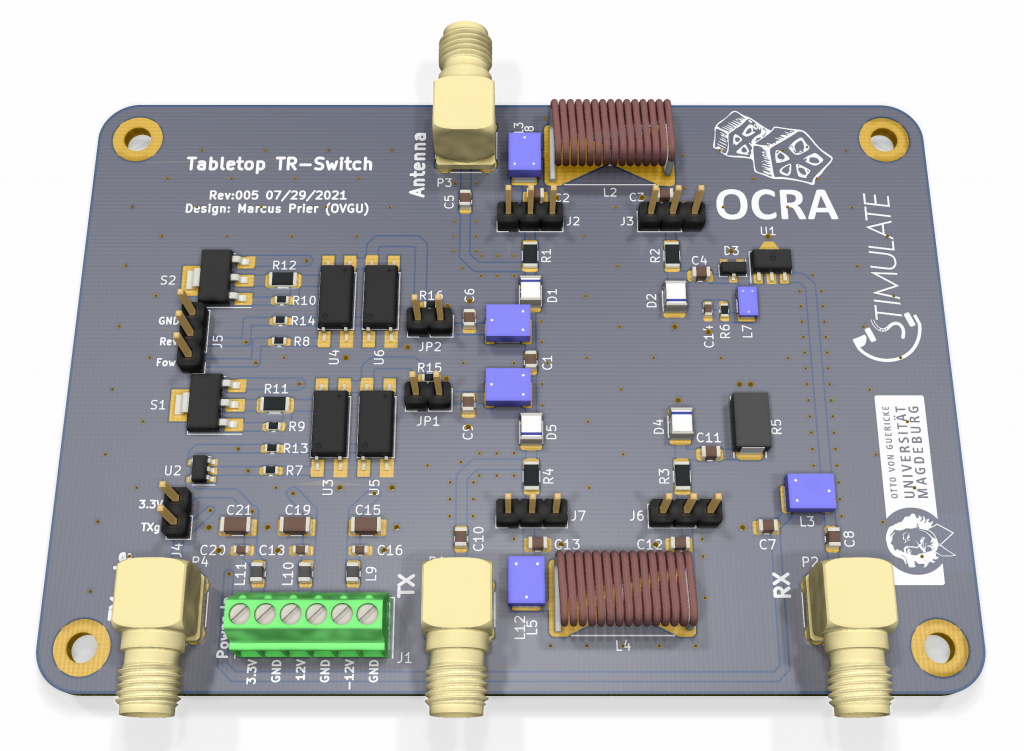
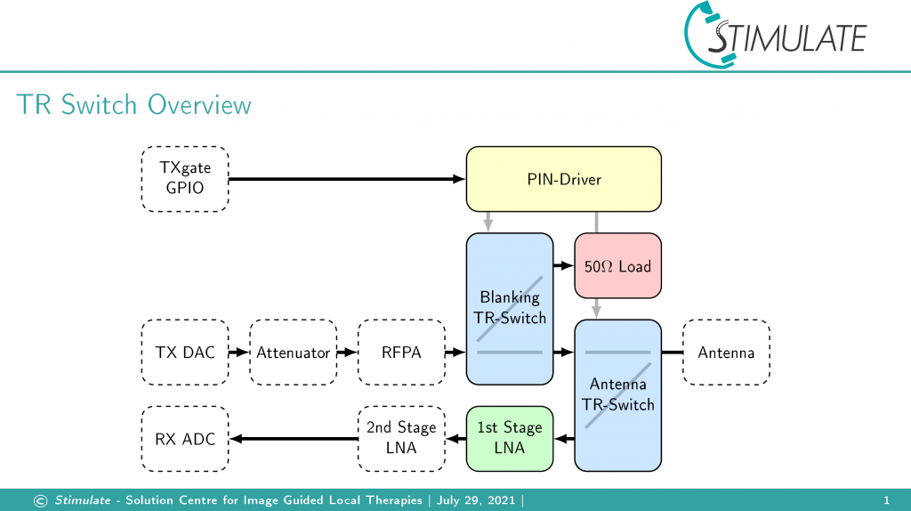
In this blog I will share my Transmit-Receive (TR) switch design for our OCRA Tabletop MRI system. As it’s a general design, it also can be used for small RF-power applications in other MRI systems. The TR-switch is used to connect the RF-coil (antenna) to the RF Power-Amplifier (RFPA) in transmit mode or the antenna to the low noise pre-amplifier (LNA) in receive mode. This is done with a classical semi-active lambda/4 PIN-diode switch, controlled by a PIN-driver. The PIN-driver controls the forward or reverse bias to some PIN-diodes in the TR-switch. The forward mode drives a controlled 100mA current to set the PIN-diodes to low-impedance, while the reverse mode set the PIN-diodes to high-impedance. The reverse mode can be powered with up to -12V for faster PIN-diode discharge. This allows for faster TX-to-RX switching times. The necessary control signal is a simple LVTTL (3.3V) “TXgate” that is low on receive and high on transmit.
Specs:
- For up to about 60W RF peak power
- Tuneable from about 1MHz up to about 150MHz
- Extra TR-switch for RFPA noise blanking
- Powered by 3.3V, 12V and optional -12V
- Controlled with a LVTTL TXgate
- Integrated 1st stage low noise amplifier
- Semi-active design with PIN-driver
- Optional reverse bias
Assembly
Some elements need specially chosen to the measuring frequency. For our OCRA Tabletop MRI system the Larmor-frequency is about 11.3MHz. An example is given here and these parts can be found also in the Materiallist.
RF-chokes (how to choose):
Footprint: Coilcraft 1812CS
https://www.coilcraft.com/en-us/products/rf/ceramic-core-chip-inductors/1812-(4532)/1812cs/
- As high as possible
- Self-resonance frequency of the RF-choke about 10 to 20MHz (short, but not too short, as of the component tolerances) above your measuring (Larmor) frequency
- Our Tabletop (example): 11.3MHz > SRF 20-30MHz > 1812CS-273 (27µH, SRF = 30MHz)
Pi Element (calculate and how to choose)
L=Z0/(2 pi f0)
C=1/(2 pi f0 Z0)
Z0 = 50 Ohms
Our Tabletop (example): f0 = 11.3MHz. This gives L = 700nH and C = 280pF.
For the capacitors choose the closest value in the E12 or better E24 series. Component parameters arameters are: 0805, 50V, 1%.
For the inductors choose Coilcraft air-coils 2929SQ, 2222SQ, 1515SQ or 1111SQ.
https://www.coilcraft.com/en-us/products/rf/air-core-inductors/square-air-core-inductors/1111sq/
Bigger coil means better quality and higher RF-power handling. So put as much of the calculated value in the biggest possible air-coil (biggest possible is 2929SQ 500nF). On small values choose the next higher coil value to the calculated value (like calculated 373nH, take the Coilcraft 2929SQ 390nF air-coil). If the air-coil covers your calculated value, you can bridge the FixCoil pads with 1206 0Ohm SMD resistors.
For our Tabletop we pick the 500nH air-coil and therefor have 200nH left. For this we pick the next higher Coilcraft fixed ceramic core inductor 1812CS or 1206CS. For our tabletop we pick the 1206CS 220nH inductor.
Easiest way for experimenting is to have the Coilcraft coil kits.
How to build, tune and test the TR-Switch
Solder almost all components to the PCB. Leave open the 1206 0Ohm resistors (R1, R2, R3 and R3). Test for shorts between the power lines, RF-lines and GND.
Tune the pi-elements: Use the test pins J2 and J3 for the antenna TR-switch pi-element and the test pins J2 and J3 for the blanking TR-switch pi-element.
Use a vector network analyser with a Coax-to-pin-header adapter cable. Measure S21 phase at your measurement frequency. Bridge the adapter cable and set the port delay offset that the phase is 0°.
Connect the adapter cable to the measuring ports (J2-J3 or J7-J6).
The phase should be slightly higher than 90° when picked the right components close to the calculated values. By stretching the air-coil you can tune the phase to exactly to 90°. If not, you need the next smaller fixed coil (change this first), or air-coil, or capacitor. Try to deviate form the calculated values as less as possible.
Tune both pi-elements. To prevent detuning you can cover the air coil in superglue. After tuning you can solder in the 1206 0Ohm resistors (R1, R2, R3 and R3).
Measure the diode voltage of about 1.1V with a multimeter between JP1(TRswitch side) – GND (J5) and JP2(TRswitch side) – GND (J5). Be aware of the right polarisation.
Connect 3.3V power and GND. Measure the voltages on J1.
Measure TXgate (Fow) and TXgate_inv (Rev) on J5. To simulate the high TXgate you can bridge J4 with a jumper.
| Mode | J4 | J5 Fow-GND | J5 Rev-GND |
| Forward | Bridged | 3.3V | 0V |
| Reverse | Open | 0V | 3.3V |
Now additionally connect 12V and (optional) -12V power. Make sure all power supply “GNDs” (when using floating outputs) are connected. Be aware of the polarisation. Measure with HighZ as the negative voltage is not regulated (reminder: PIN diode is reverse will block the current).
Measure the voltages on J1.
Measure the PIN voltages (or in forward mode currents) on JP1 (PIN-Driver side) and JP2 (PIN-Driver side) to GND (J5).
| Mode | J4 | JP1-GND | JP2 -GND |
| Forward | Bridged | 11.4V (better: regulated 100mA) | 11.4V( better: regulated 100mA) |
| Reverse | Open | -12V (0V, if not connected) | -12V (0V, if not connected) |
If all works bridge JP1 and JP2 with a jumper. Have J4 open.
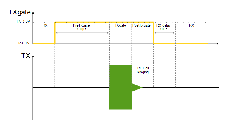
Edit1: TR switching with the TXgate
To compensate for hardware switching delays the TXgate needs to be adopted. The RX-TX switching time is long as the RF choke inductors and the PIN-diodes need to be charged. A PreTXgate (3.3V) of about 100µs needs to be set before the RF pulse. The RF pulse (still with the TXgate (3.3V)) can be of any length. After turning of the RF pulse a PostTX (3.3V) gate should be applied. This prevents stored RF energy in the coil to be discharged in the pre-amplifier path. After the RF coil ringing the TXgate can be set to RX (0V). Due to the reverse voltage the PIN current discharge is much faster. So only a RX delay of about 10µs needs to be taken into account.
TR-switch production files, BOM, parts list, fabrication plan and images can be found here:
Edit2: Low Noise Amplifier – LNA
The board works with 50Ohm input impedance low noise amplifiers in case style DF782. The circuit layout is for two Mini Circuit preamps:
f0 > 1MHz: PHA-13LN+, no components on L7, R6 and C14
f0 > 50MHz: PGA-103+, components on L7, R6 and C14
https://cloud.ovgu.de/s/D6xH63MMtBF2sqM
When downloading the files, you declare to cite us as creator of the Tabletop TR-switch when using in your projects or publications (Marcus Prier, Forschungscampus STIMULATE, Otto-von-Guericke University Magdeburg). You are not allowed to remove logos or references.
If you have questions about the OCRA Tabletop TR-switch or interest in a preassembled PCB, Tabletop and OCRA components or even a whole OCRA Tabletop system contact me via marcus.prier@ovgu.de.
Best Regards
Marcus
Thanks for sharing, Marcus, that’s just what we are looking for. We constructed and test the t/r switch board following the document you shared and find the rise time of the transimit signal is about 10us, fall time 8.6us, which is a little too long for our application, since our RF signal duration is about 10us. Have you also obtain the same switch time? Have you any suggestions about faster switch time? Looking forward to your reply.
Hi,
the RX-TX and TX-RX times depend on the opto-transistors of the PIN-Driver, but more on the applied load. As the RF chocke inductors and the PIN-diodes have charging times. Short pulses are not a problem at all. You just need to implement the switching times in the TXgate signal form. These TXgate extensions are the Pre- and PostTXgate signals.
I will edit the blog post to explain this.
Best,
Marcus
Thanks for the help from Marcus, it is the problem of RF choke inductors and the PIN-diodes charge effect. Following the new instruction of blank delay, now our application work perfect. Nice work~