Hello OCRA Community,
I would like to introduce you to one of the core elements of our OCRA Tabletop MRI console, the OCRA1. It’s a peripheral printed circuit board (PCB) that extends a Red Pitaya to a basic MRI console. All its components are controlled with the Serial Peripheral Interface (SPI) bus given by the RP GPIO pins.
The Red Pitaya fuses a microcontroller with a field-programmable gate array (FPGA). It coordinates the image acquisition by generating RF pulses (TX) and control signals for the transmit-receive switch (TXgate). The received magnetic resonance signal, generated at the RF coil in the system, is sampled at an RF input channel through the integrated ADC (RX). Also, general-purpose in- and outputs (GPIO) are programmed to control the OCRA1 board and handle multiple SPI busses for additional components.
The OCRA1 is based on design ideas, requirements, and first component tests, that were made by Thomas Witzel at the Martinos Center in Boston. From this I (Marcus Prier) designed the OCRA1 schematic and PCB at the Forschungscampus STIMULATE (Otto-von-Guericke University Magdeburg).
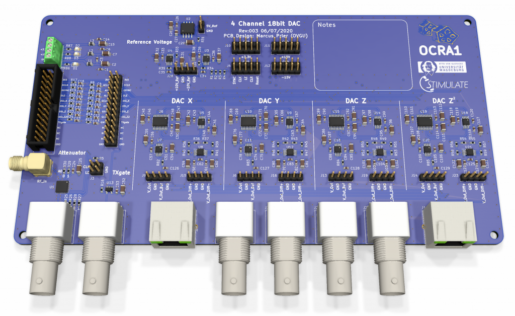
Image1: OCRA1 Revision 003.
The OCRA1 consists of:
- 4 18bit DACs; driven by a ±10V reference voltage; with single-ended and differential output. The DACs generate gradient pulses and offsets for shimming. For the image acquisition, three gradient coils need to be controlled for the dimensions X, Y, and Z. A fourth channel Z² serves for further field homogenization by higher-order shimming or can be used by systems with a B0 channel.
- 1 RF Attenuator For adjustments on the power of a radio frequency transmit pulse.
- 1 TXgate Buffer/Schmitt Trigger to decouple and filter the switched RF infrastructure from the noisy Red Pitaya GPIO
18bit DAC
The DAC is based on the AD5781B and its evaluation board. The DAC is driven with ±15V and 3.3V supply voltage. To achieve stable shimming and precise gradient waveforms this DAC has a ±0.5 LSB long-term linear stability. A stable voltage reference is necessary to archive good output stability. Common gradient amplifier inputs are in the range of ±10V. So a ±10V reference voltage is needed as Limits for the DAC. Inspired by the evaluation board schematics for the AD5781B, the ±10V reference voltage is generated via a 5V voltage reference (here we use an LT1072) and two gain-2 buffers and one inverting OP-amp. This voltage reference is shared by all 4 channels. The DAC uses a common SPI bus clock (DCLK), an SPI bus synchronization (DSYNC), and a latch signal (DLE) generated by the RP. Each channel has its own RP SPI data signal line (DSI_X, DSI_Y, DSI_Z, and DSI_Z2). The DAC output is single-ended and buffered. There is an optional low pass filter to reduce the DAC switching/stepping harmonics. In addition, as most gradient amplifiers have a differential (symmetrical, ground independent) input, a fully differential amplifier (THS4131) is provided in parallel to the single-ended output. With its resistor combination, the span of the differential signal is set up to 20V (1:1 to the ±10V of the single ended outputs).
RF Attenuator
The RF attenuator is based on a PE43704. It’s a 7bit attenuator with 0.25dB stepping up to 31.75dB in the range of 9kHz-8GHz. It is 3bit addressable, enabling the capability to add more attenuators to its bus lines. The address is set by three 0Ohm resistors (A0, A1, and A2). It’s driven by 3.3V and uses its own SPI bus clock (ACLK), a letch signal (DLE), and an SPI data signal line (ASI) from the RP.
TXgate Buffer
The TXgate is an LVTTL signal (3.3V) generated by one of the RP GPIOs. In general, the receive mode is low state to reduce digital noise in the RF chain. Observations show that the RP GPIO/Bus lines are usually coupling a bit and so induce noise to the TXgate. To decouple and filter the TXgate line a Schmitt Trigger (SN74LVC1G17) is used. Optionally this IC can be bypassed with a 0Ohm resistor.
Peripherals
The OCRA1 has supply voltage status LEDs, test points, jumpers, and additional headers for busses, supply- and reference-voltages as test points and outputs. This enables easy debugging and extensibility.
It has an optional low pass filter for all RP bus and GPIO lines. This reduces overall high frequency switching harmonics on the OCRA1 board. All bus lines are connected via a single flat ribbon cable from the RP.
Via the bus test header pins, it’s also possible to daisy chain the busses to external boards. This functionality enables us to connect multiple OCRA1 boards or additional SPI-driven hardware.
The DAC, TX and TXgate outputs are BNC connectors for easy testing and monitoring with oscilloscopes or VNAs/spectrum analyzers. In addition, the DAC outputs are summarized in RJ45 connectors. One for single-ended output signals and the other one for differential mode output.
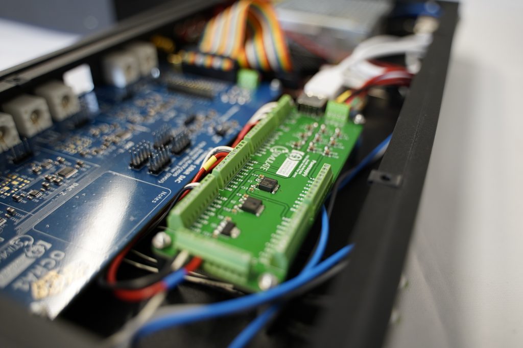
Image2: Red Pitaya, OCRA1 and a power-supply/distributor in a 19” case.
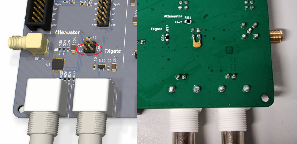
Edit1: Attenuator reset fix
In rare cases SPI bus coupling can reset the attenuator at the start of a sequence. To suppress the coupling peaks that trigger the reset a 1nF capacitor from ALE to GND next to the attenuator IC is a simple fix. A good place to solder the decoupling capacitor is the backside of the attenuator bus line test header. The location is shown in image3. The part number for the capacitor is C315C102J3G5TA.
The OCRA1 production files, BOM, parts list, fabrication plan and images can be found on:
https://cloud.ovgu.de/s/9Ek5xczgPdciqHP
When downloading the files, you declare to cite us as creator of the OCRA1 when using in your projects or publications (Marcus Prier, Forschungscampus STIMULATE, Otto-von-Guericke University Magdeburg). You are not allowed to remove logos or references.
If you have questions about the OCRA1 or interest in a preassembled PCB or even a whole OCRA console contact me via marcus.prier@ovgu.de.
Best Regards
Marcus, David and Ivan
0 thoughts on “OCRA1 – SPI controlled 4 channel 18bit DAC and RF Attenuator”